Why scientists create vdW heterostructures from 2D materials
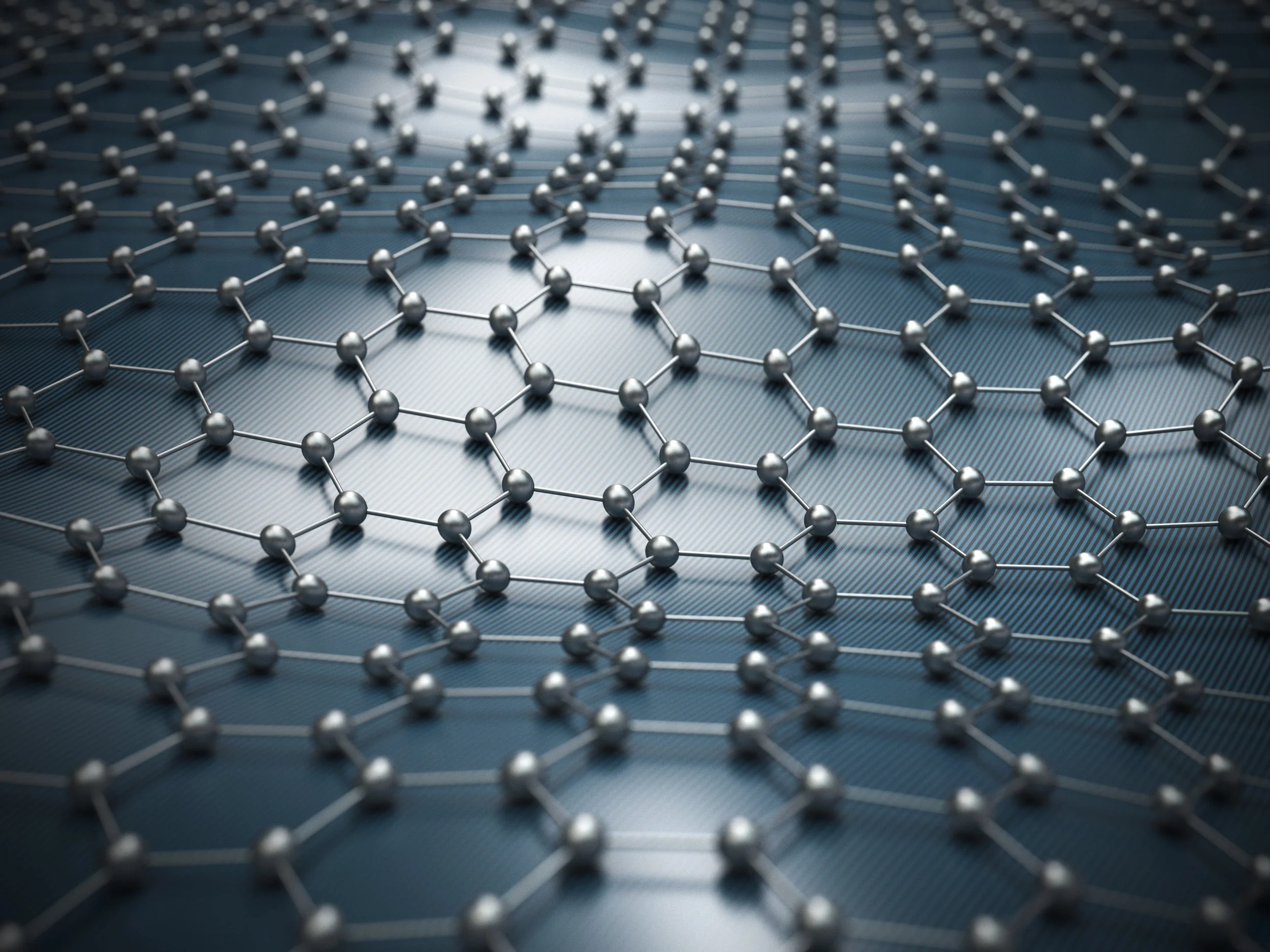
Since the isolation of graphene in 2004, there has been a lot of effort to produce it synthetically, and with great success. Whilst there are many types of graphene, the chemical vapour deposition process (CVD) is know for being the best way of producing single-layer graphene. Since graphene, there have been many more single-layer 2D materials created—both in the academic laboratory and at a commercial level. Whilst some of these materials show similar properties to graphene, some have opposite properties, and some lie in between the two. These most common examples of other conductive 2D materials include some of the transition metal dichalcogenides (TMDCs), whereas hexagonal boron nitride (h-BN) is the most common electrically insulating material related to graphene.
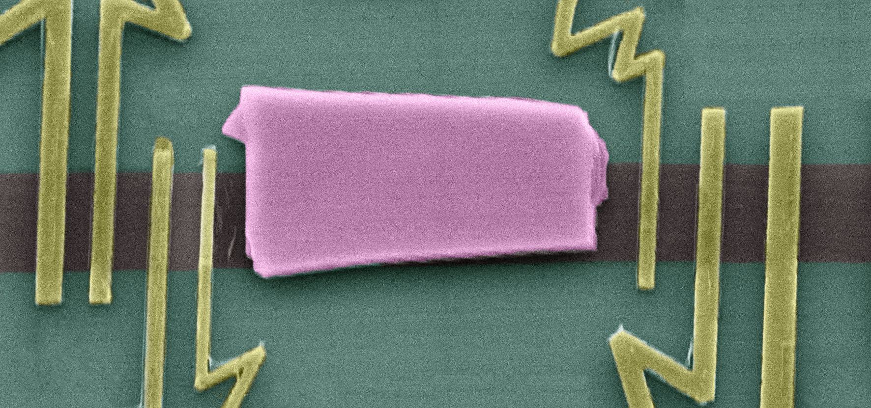
So, what are vdW heterostructures. For those not familiar with shortened nomenclature, ‘vdW’ is shorthand for van der Waals, and ‘hetero’ is a prefix which literally means different. Therefore, vdW heterostructures are materials which are created by stacking different single-layer 2D materials on top of each other, where they are simply held together by the van der Waals forces between the layers. It is a very similar principle to graphite, where each individual layer of graphene is held in place by vdW forces between the layers. However, graphite is not a heterostructure because all the layers are made up of the same material.
There are two main ways of producing vdW heterostructures. The oldest, but slowest method is the direct stacking of individual layers (in the form of flakes) on top of each other until the desired heterostructure is formed. However, one of the biggest growing methods nowadays is the use of direct deposition techniques, such as CVD, which starts from nothing and grows each layer individually (one on top of the other) until the heterostructure is complete.
So Why Fabricate vdW Heterostructures?
The ability to combine different 2D materials together brings about properties and synergistic effects that are not seen in homostructures or individual layers. Building heterostructures out of 2D materials is a method that yields more possibilities than any other growth method, but the utilisation of graphene with either h-BN or TMDCs is by far the most popular routes, but can include metals, other semiconducting materials and layered organic materials as well. But, given the fact there are over 100 TMDCs in existence today, these two main routes offer an endless number of heterostructure possibilities on their own.
So, on one hand, the creation of heterostructures is a way of creating a material with the ideal electronic and topological properties required for a certain application. These can range from the need to create a material with certain dielectric properties, to a molecularly smooth surface (i.e. no dangling bonds), and to using one 2D material to increase the charge carrier mobility of another 2D material (compared to a single layer). These are just a few examples of how the properties can be tailored for certain applications, and in ways that you don’t see with a single layer or a homostructured material. A couple examples of specific devices that benefit from this arrangement include optically active transparent electrodes using graphene and semiconductor layers and using h-BN to significantly improve the properties of graphene transistors (an example of increasing the charge mobility of the ‘active’ material in a device).
Aside from creating materials to fit a certain requirement, incorporating 2D materials into heterostuctures is a way of analysing how different 2D materials behave in different environments and when paired with other materials (as many 2D materials are going to be used in conjunction with other materials for many commercial applications). Some of the properties that can be analysed via heterostructure incorporation include how the presence of another crystalline material changes the structural composition of the 2D materials(s), how these materials redistribute their charges when they come together, and the drag effects between different 2D materials. Heterostructures also provide a way observing certain phenomena in, and between, 2D materials, such as electron tunnelling, topological currents and the Hofstadter butterfly effect.
Written by Liam Critchley.