Search for advanced 2D materials aided by robots

A Japanese research team has developed a robot for the automated assembly of two-dimensional crystalline nanomaterials.
Researchers at the University of Tokyo, Japan, have created a robot that can automatically assemble two-dimensional (2D) crystalline materials. They published their findings in Nature Communications.
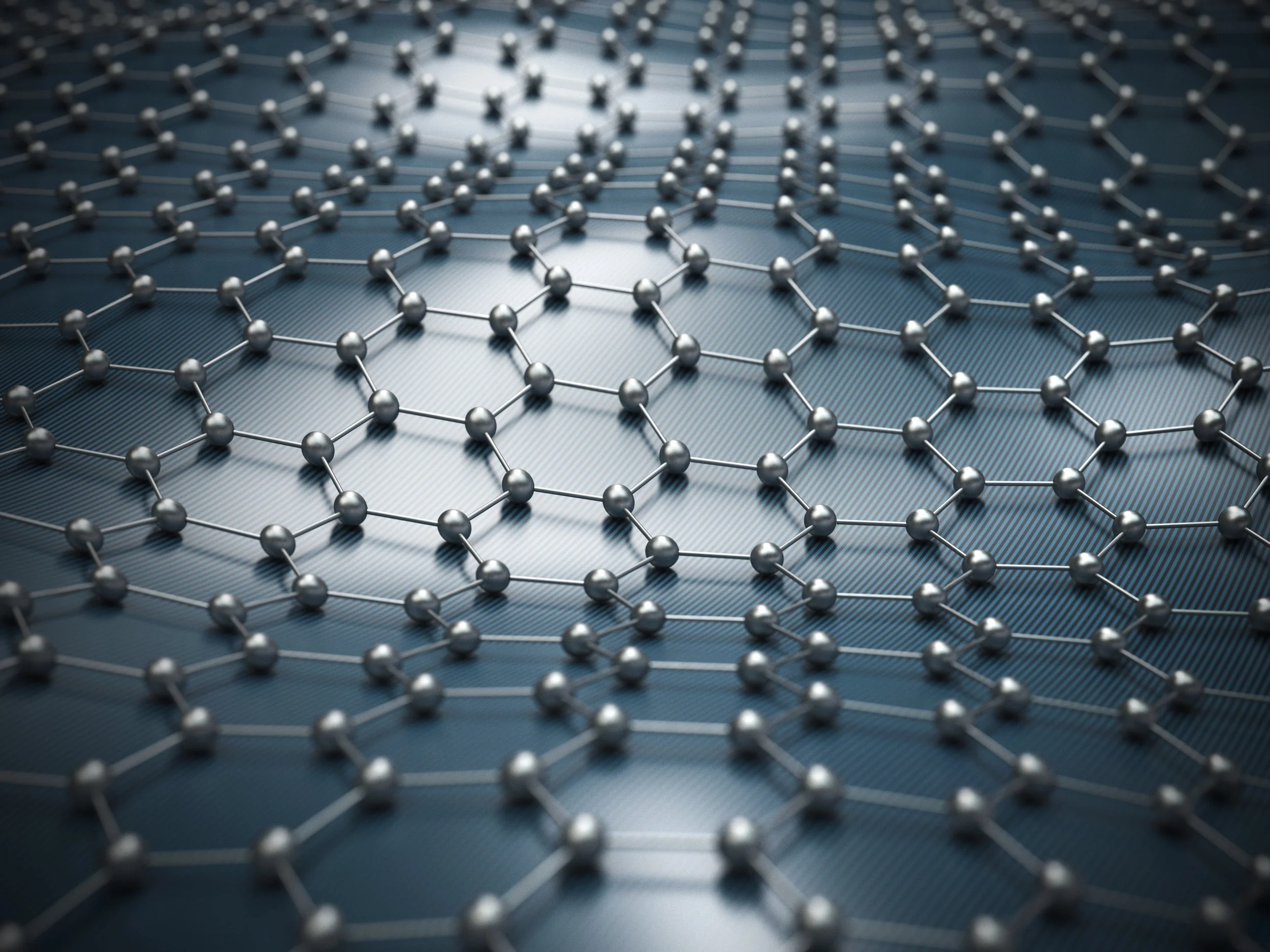
van der Waals heterostructures, which are assemblies of atomically thin 2D crystalline materials, are of interest in nanotechnology for their attractive conduction properties. A representative 2D semiconductor is graphene, which consists of a honeycomb lattice of carbon atoms that is just one atom thick.
The development of van der Waals heterostructures has been restricted by the complicated and time-consuming manual operations required to produce them. Currently, 2D crystals are obtained by exfoliation of a bulk material and need to be manually identified, collected and then stacked by a researcher to form a van der Waals heterostructure.
In this study, a Japanese research team led by Dr. Satoru Masubuchi at the University of Tokyo has solved this issue by developing a robot that greatly speeds up the collection of 2D crystals and their assembly into van der Waals heterostructures. The robot consists of an automated high-speed optical microscope that detects crystals, recording the positions and parameters of the crystals in a computer database.
Customized software is used to design heterostructures based on the information in the database. The robot then assembles the desired heterostructure layer by layer.
“The robot can find, collect and assemble 2D crystals in a glove box,” study first author said Masubuchi. “It can detect 400 graphene flakes an hour, which is much faster than the rate achieved by manual operations.”
When the robot was used to assemble graphene flakes into van der Waals heterostructures, it could stack up to four layers an hour with just a few minutes of human input required for each layer.
The robot was used to produce a van der Waals heterostructure consisting of 29 alternating layers of graphene and hexagonal boron nitride, another common 2D semiconductor. This is more than double the record layer number of a van der Waals heterostructure produced by manual operation, which stands at 13.
“A wide range of materials can be collected and assembled using our robot,” said co-author Professor Tomoki Machida of the University of Tokyo. “This system provides the potential to fully explore van der Waals heterostructures.”
The article can be found at: Masubuchi et al. (2018) Autonomous Robotic Searching and Assembly of Two-dimensional Crystals to Build van der Waals Superlattices.
Photo: Satoru Masubuchi/University of Tokyo.