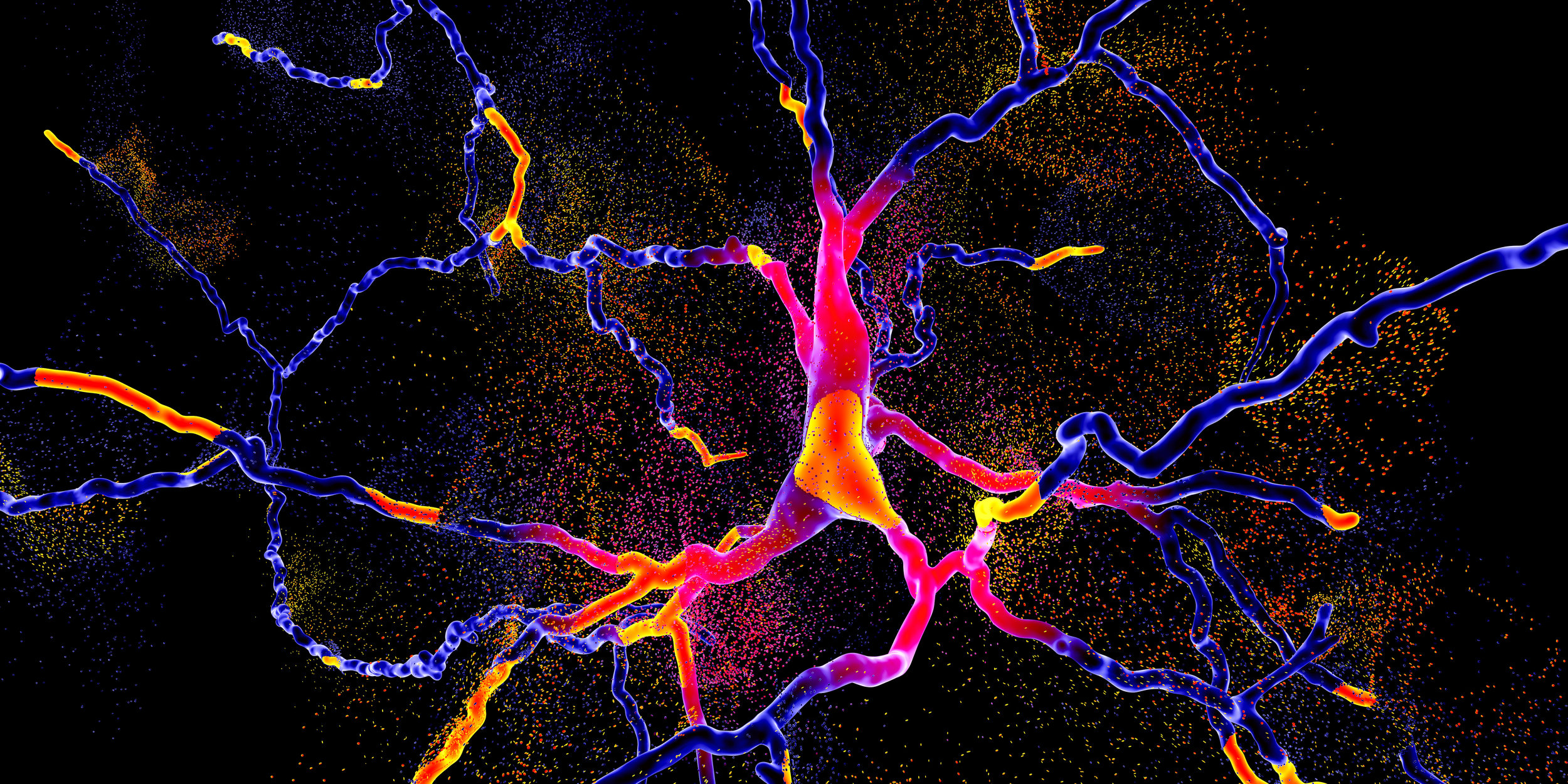
The quantum world of nanotechnology

As quantum technologies operate through the exploitation of matter at very small scales, they are dependent and underpinned by advances in the field of nanotechnology.
The world of nanotechnology is an interesting space, and one that is filled with so much variety. Many people hear about how nanotechnology can be used in quantum computing and other similar electronic technologies, but how many people understand the quantum world of nanotechnology? This article aims to shed some light on the basic principles of quantum nanotechnology.
There are two fundamental principles at the core of nanotechnology – The first is that the smaller you make the material, the greater the relative surface area of the material; and the second is the loss of bulk properties in lieu of quantum phenomena when you get to such a small scale.
It all starts with a box…
And by a box, I mean a particle in a box. Quantum nanotechnology is based around the principle of electron tunnelling. The basic theory is that a particle confined to a one-dimensional box cannot escape unless the electron tunnels its way out of the confinement. This is a phenomenon only exhibited by quantum materials and is not seen with any bulk materials. This principle can be extended to incorporate all 3-dimensions – the so-called particle in a three-dimensional box. The amount of electron confinement introduced to a material will determine its dimension – as quantum dimensions are more relative the electron confinement (and in how many dimensions the electrons act in) than the atomic spatial arrangement.
Quantum dots
Quantum dots are likely to be the most known quantum structure in this article. The interesting thing about quantum dots, is that electronically, they are confined in all 3-dimensions, so they are classed as zero-dimensional materials.
Quantum dots are an interesting class of materials, and many of them luminesce (which is usually tuneable). They are semiconducting in nature and are often referred to artificial atoms because they possess discrete electronic states – i.e. the states can only take certain values of energy (unlike bulk materials). Quantum dots are now gaining a lot of interest across many applications, and some research now focuses on the phenomena of double quantum dots.
Quantum wires
Otherwise known as nanowires, quantum nanowires are an electrically conductive one-dimensional structure with electrons confined in two dimensions. They are referred to as ‘wires’ because the electron movements are confined to one transverse direction, i.e. along the wire, making their mode of operation similar to conventional wires. They are used to pass electrons in electronic devices, or sensing devices, but can only be used a certain energy levels, because their bands are also discrete. One major benefit of quantum wires is their high aspect ratio, where the length of the wire can be up to 1000 times greater than their width.
Quantum wells
Quantum wells are only confined in one direction, so electrons can tunnel in two directions. This enables quantum wells (also known as potential wells) to be connected to each other under the right conditions.
Quantum wells are usually seen in semiconducting materials and the geometry of the well forces the particles into a planar axis. Quantum wells are a phenomenon created by the discrete energy bands of holes and electrons in semiconducting materials. These discrete energy levels lead to sub-bands with the material, where each well is not connected to each other and the electrons cannot tunnel out.
However, there are cases where the distance between potential wells is not sufficient to block all electrical contact between wells. The electrons can then tunnel and link the potential wells together, creating a ‘superlattice’. These superlattices contain minibands which run the length of the connected potential wells, meaning that electrons can easily travel between wells and enables the superlattice to exhibit excellent charge carrier properties, and in some cases, superconductivity.
Applications
There are too many applications of quantum materials to go into sufficient detail here. However, there will be another article coming shortly focusing on these quantum applications. But, for now, here is a list of some of the areas that quantum nanotechnology is involved in: transistors, solar cells, LEDs, diode lasers, quantum computing, saturable absorbers, thermoelectric devices and medical imaging, to name a few.
Funding
The UK Government’s Industrial Strategy Challenge Fund (ISCF) was announced last year to provide funding and support to UK businesses and researchers and forms part of their commitment to a £4.7 billion increase in R&D over the next four years. One of the 14 key industrial challenges identified is for quantum technologies, where they have pledged up to £20million of funding to develop prototypes, having recognized this could have a significant impact across a number of their challenge areas.
It is believed the emerging field of quantum technologies could lead to new products in areas such as medical devices, advanced sensors and secure communication systems. Although much of the work is in the lab environment, the funding aims to advance the commercialisation of quantum technologies through collaboration with businesses. This new funding commitment expands on the £25 million the government has already invested in a number of Innovate UK quantum technology funding programmes since 2014.
Applying for funding can be complex and time-consuming and so businesses should seek guidance from specialists advisors. Through their knowledge of the breadth of government funding, a specialist in this field can also ensure a business has considered all options available, including R&D tax relief schemes, and has chosen the most suitable for them.
For further information, or for advice on the funding options available to your business, please contact us.
Written by Tariq Ahmad.
Tariq is a Manager in the Moore Stephens’ Innovation & Technology Group (ITG) specialising in the delivery of R&D tax relief claims and grant funding applications for clients over a range of industries including engineering, manufacturing, materials, biotechnology, environmental and software.
Tariq holds a PhD in Semiconductor Nanotechnology from the Hitachi-Microelectronics Research Institute at the University of Cambridge. He also has many years’ experience as an R&D project engineer for an international scientific instrumentation company, specialising in low temperature cryogenic and superconducting magnet systems. Through his career he has gained experience of cutting edge research globally and worked with many leading Universities and research institutes. His particular R&D interests include nanotechnology, quantum technologies, graphene and superconductivity.