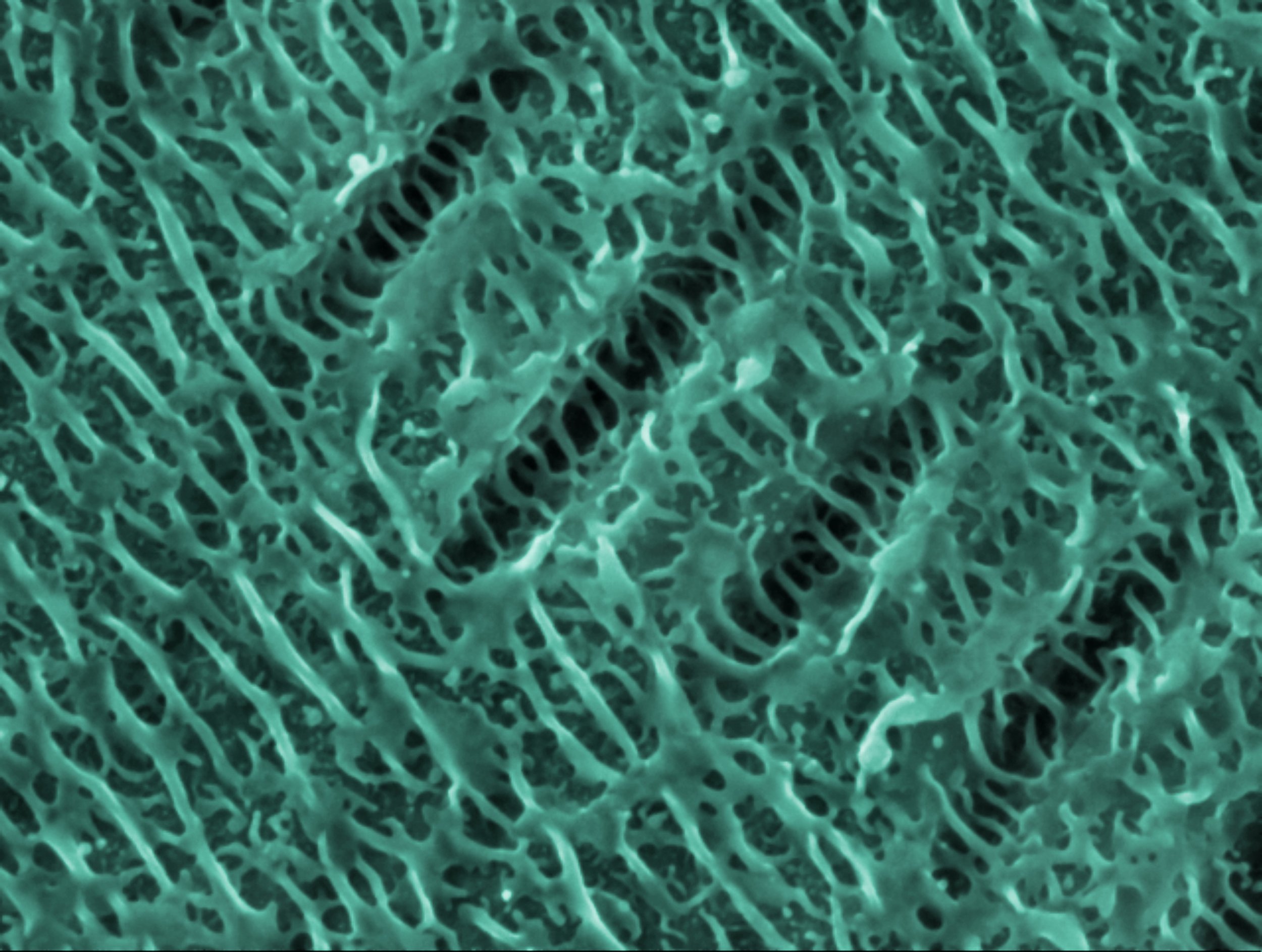
A New Era in Electronics with Mass Production of Metal Nanowires

In recent years, the demand for smaller, more efficient, and faster electronic devices has dramatically increased. This is particularly evident in areas such as consumer electronics, renewable energy, and medical technology, where advancements rely heavily on miniaturisation and the enhancement of device performance.
As a result, researchers are constantly searching for new materials and methods that can meet the growing expectations of the industry. One such material, metal nanowires (NWs), holds significant promise due to their unique properties, but producing them at a large scale has presented considerable challenges. To address this, a group from Nagoya University in Japan has developed an innovative technique that could revolutionise the mass production of NWs, unlocking their potential for widespread use in next-generation electronics.
The research group, led by Yasuhiro Kimura at the Nagoya University Graduate School of Engineering, has proposed a novel method for growing metal nanowires that could make their mass production both feasible and cost-effective.
Until now, the use of metal nanowires in commercial applications has been constrained by the difficulty of producing them in large quantities while maintaining the high levels of quality and purity required. Nanowires are incredibly small, necessitating precise manufacturing techniques that manipulate matter at the atomic level.
This process is particularly complex when it comes to metals, as atoms need to be transported in a gas phase state, a task that has proven challenging due to the properties of metals.
To tackle this issue, the researchers introduced a groundbreaking method that uses atomic diffusion in a solid phase, aided by ion beam irradiation. This technique allows for the creation of aluminium nanowires from single crystals in a much more controlled and scalable manner.
Atomic diffusion refers to the movement of atoms or molecules from regions of high concentration to areas of lower concentration, driven by changes in stress under the influence of heat. The application of ion beams during this process coarsens the crystal grains on the surface of a thin aluminium film, altering the stress distribution. This adjustment in stress guides the flow of atoms, which then form the building blocks for the nanowires, allowing them to grow in specific, targeted locations.
The process itself is relatively simple, involving just three key steps: depositing a thin film of aluminium onto a substrate, irradiating the film with ion beams, and applying heat. Once the heat is applied, the atoms within the film move upwards from the finer grains at the bottom towards the coarser grains at the top, promoting the rapid growth of nanowires.
According to Kimura, this new method significantly increases the density of nanowires produced. "We increased the density of aluminium NWs from 2×10⁵ NWs per square cm to 180×10⁵ per square cm," Kimura stated. "This achievement paves the way for bottom-up metal NW growth methods, which have so far been grown only accidentally and in small quantities. It can also be extended to other metals in principle."
The ability to produce such high densities of nanowires opens up a host of possibilities for their use in various fields. Aluminium nanowires, for example, possess desirable characteristics such as a large surface area, high mechanical strength due to their single-crystal structure, and excellent resistance to oxidation, which makes them ideal candidates for use in sensing devices and optoelectronics.
Their unique features allow them to serve as critical components in devices that require high performance on a very small scale. Kimura expressed optimism about the broader applications of the technology, noting, "We realised mass growth of forest-like metallic NWs using only three key processes: thin film deposition on a substrate, ion beam irradiation, and heating."
This breakthrough could have significant implications for industries that depend on high-performance nanodevices, such as gas sensors, biomarkers, and optoelectronic components. These devices require materials that can withstand the stresses of miniaturisation while maintaining high functionality, and metal nanowires are ideally suited to meet these demands.
However, the inability to produce nanowires in large quantities has been a major obstacle, limiting their practical use. Kimura highlighted the importance of overcoming this hurdle, stating, "Our technique solves the urgent need to establish mass production methods, especially in the production of high-performance nanodevices such as gas sensors, biomarkers, and optoelectronic components."
The successful development of this method not only solves a longstanding issue in nanowire production but also provides a scalable and efficient approach that could be applied to other metals. The researchers believe that this technique could lead to further innovations in the electronics industry, particularly in the development of devices that rely on nanotechnology for enhanced performance. As industries continue to push the boundaries of what is possible with miniaturisation and advanced materials, the ability to mass produce high-quality nanowires could prove to be a game changer.
In conclusion, the technique devised by Kimura’s team offers a promising solution to the problem of metal nanowire production, potentially unlocking their full potential for use in next-generation electronic devices. By simplifying the manufacturing process and increasing the density of nanowires produced, this breakthrough paves the way for their widespread application in various high-tech industries. The research represents a significant step forward in the field of nanotechnology, offering new opportunities for innovation and advancement.
Author:
Kate Sivess-Symes
Content Producer and Writer


