Cheaper chips with nanotube alignment process?

Two chemists from the University of Waterloo in Canada say they have made it easier to produce faster and cheaper semiconductors. In their work, the chemists have found a way to not only control the orientation of single walled carbon nanotubes deposited on a surface, but also to select their size. This, they claim, could allow carbon to be used for semiconductors, rather than silicon. In turn, this will reduce device size and increase operating speed.
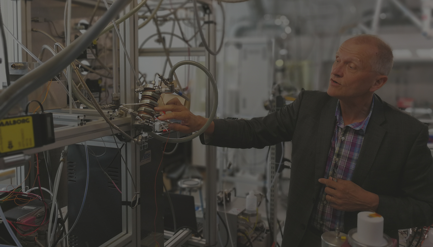
“We’re reaching the limits of what’s physically possible with silicon-based devices,” said Professor Derek Schipper, pictured. “Not only would single-walled carbon nanotube-based electronic devices be more powerful, they would also consume less power.”
Called the Alignment Relay Technique, the process relies on liquid crystals to pass orientation information to a metal-oxide surface. Small molecules called iptycenes then bond to the surface, locking the orientation pattern into place. Their structure includes a small ‘pocket’ large enough to fit a certain size carbon nanotube that remains after washing.
“This is the first time chemists have been able to externally control the orientation of small molecules covalently bonded to a surface,” said Prof Schipper. “We’re not the first to come up with potential solutions to work with carbon nanotubes, but this is the only one that tackles both orientation and purity challenges at the same time."
Prof Schipper added the approach is from the bottom up, with organic chemistry used to design and build a molecule which then does the hard work.
“Once you’ve built the pieces, the process is simple,” Prof Schipper contended.
The method is said to contrast with self-assembly techniques, which rely on the design of suitable molecules that fit together snugly. The Waterloo process is said to be controlled at every step, including the size of the iptycene ‘pocket’.


