Cleaning nanotubes improves their efficiency

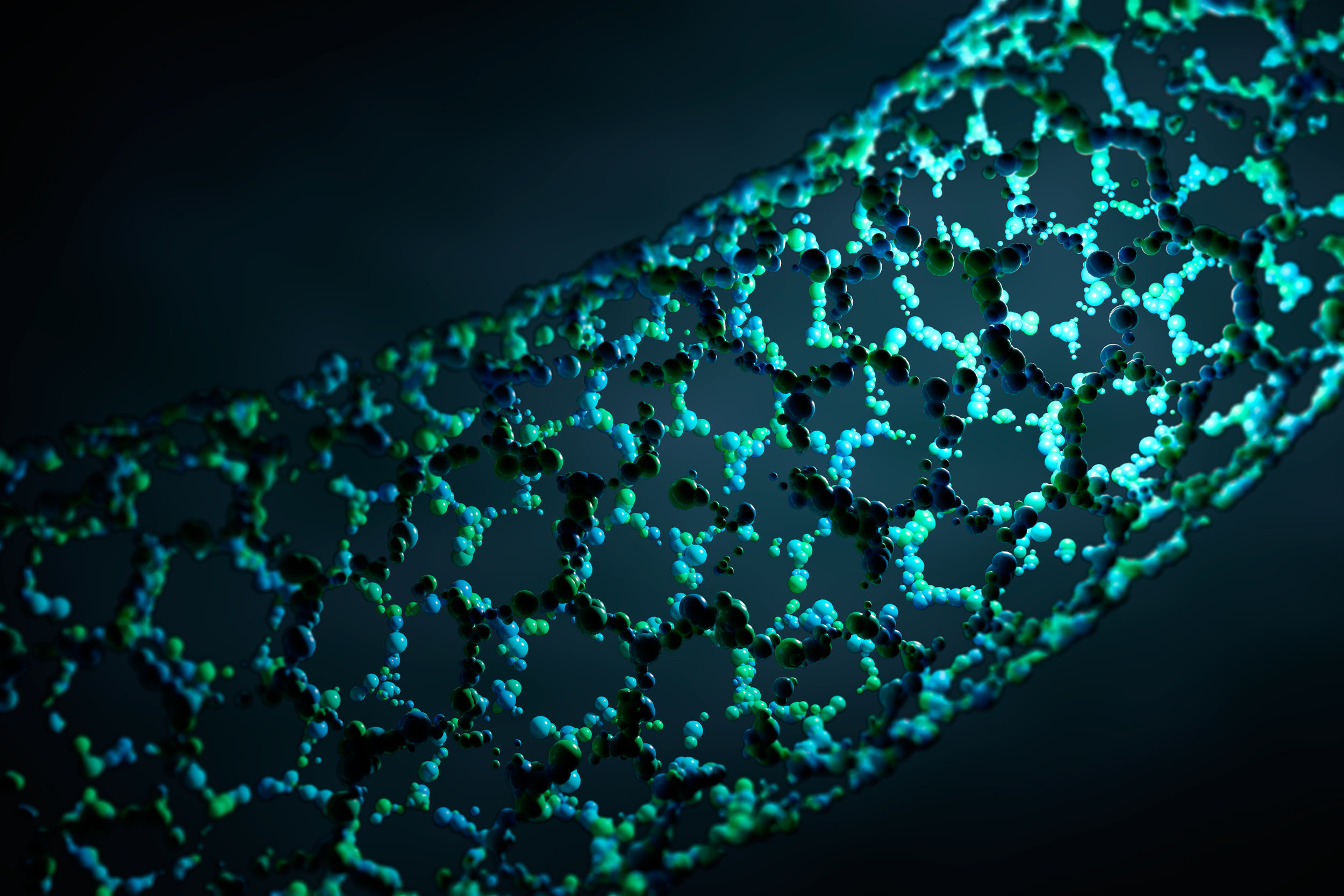
Researchers from Rice University in the US and Swansea University in the UK have demonstrated how the performance of nanoscale devices can be improved by decontaminating the carbon nanotubes they use. Their study identified how best to clean nanotubes and also why their electrical properties have traditionally been so problematic to measure.
As with standard wires, semiconducting nanotubes become more resistant to current along their length. However, measuring the conductivity of nanotubes has never been straightforward, so the team investigated the basic science underlying the variability. They found that contaminants that are difficult to get rid of, such as residual iron catalyst, carbon and water, can affect the findings of conductivity tests, and that burning away such contaminants could offer new possibilities for nanotubes in nanoscale electronics.
“If nanotubes are to be the next-generation lightweight conductor, then consistent results, batch-to-batch and sample-to-sample, are needed for devices such as motors and generators as well as power systems”Andrew Barron
As reported in the journal Nano Letters [Barnett et al. Nano Lett. (2017) DOI: 10.1021/acs.nanolett.7b03390], multiwalled carbon nanotubes of between 40 and 200 nanometers in diameter and up to 30 microns long were produced, before they were either heated in a vacuum or bombarded with argon ions to clean their surfaces. The team tested single nanotubes by touching them with two tungsten probes attached to a scanning tunneling microscope to assess the amount of current passing through the material.
As expected, for clean nanotubes the resistance became increasingly strong as the distance increased. However, the measurement is skewed when the probes encounter surface contaminants, as they increase the electric field strength at the tip. When measurements were taken within 4 microns of each other, areas of depleted conductivity caused by contaminants overlapped, further affecting the results. Heating the nanotubes in a vacuum above 2000C lessened the surface contamination, but not sufficiently to eradicate the inconsistency. In addition, argon ion bombardment cleaned the tubes but meant there were more defects that degrade conductivity. It was found that vacuum annealing nanotubes at 5000C did reduce contamination sufficiently to measure resistance accurately.
If the source nanotubes are decontaminated, it should be possible to enable the required conductivity by placing the contacts in the correct spot. If contacts on a nanotube are less than 1 micron apart, the electronic properties of the nanotube was shown to change from conductor to semiconductor because of overlapping depletion zones, which shrink but remain present in clean nanotubes, a potentially limiting factor for the size of nanotube-based electronic devices. As researcher Andrew Barron said, “If nanotubes are to be the next-generation lightweight conductor, then consistent results, batch-to-batch and sample-to-sample, are needed for devices such as motors and generators as well as power systems”.


